
Terahertz imaging for industrial inspection
Revolutionizing Non-Destructive Testing with Terahertz Imaging
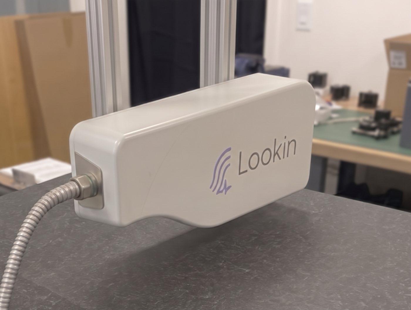
We engineer cutting-edge terahertz scanners designed for non-invasive, non-contact industrial quality inspection. Our systems deliver an unprecedented 1000x enhancement in dynamic range and throughput over conventional terahertz time-domain spectroscopy/imaging solutions, enabling faster, more sensitive, and more accurate quality control across advanced manufacturing sectors. Our scanners have been deployed for nondestructive testing and evaluation across the energy, semiconductor, aerospace, and pharmaceutical industries.
- 1000x Higher
- dynamic range and throughput over conventional systems
- Non-contact
- non-invasive, non-destructive inspection
- In-line
- real-time quality control on the production line
Technology
Why Lookin's Terahertz Scanners?
Time-Domain Imaging
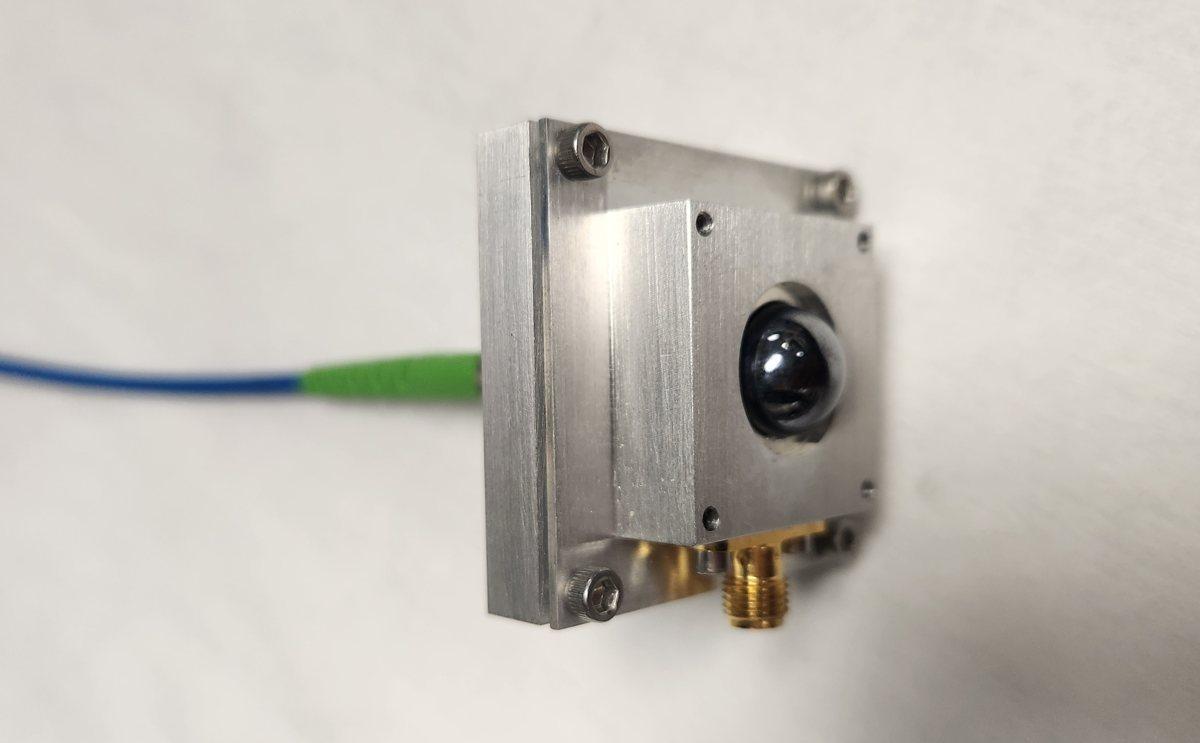
Sub-picosecond terahertz pulses record a complete temporal waveform at every point, not just an intensity value.
Multi-Pixel Solutions
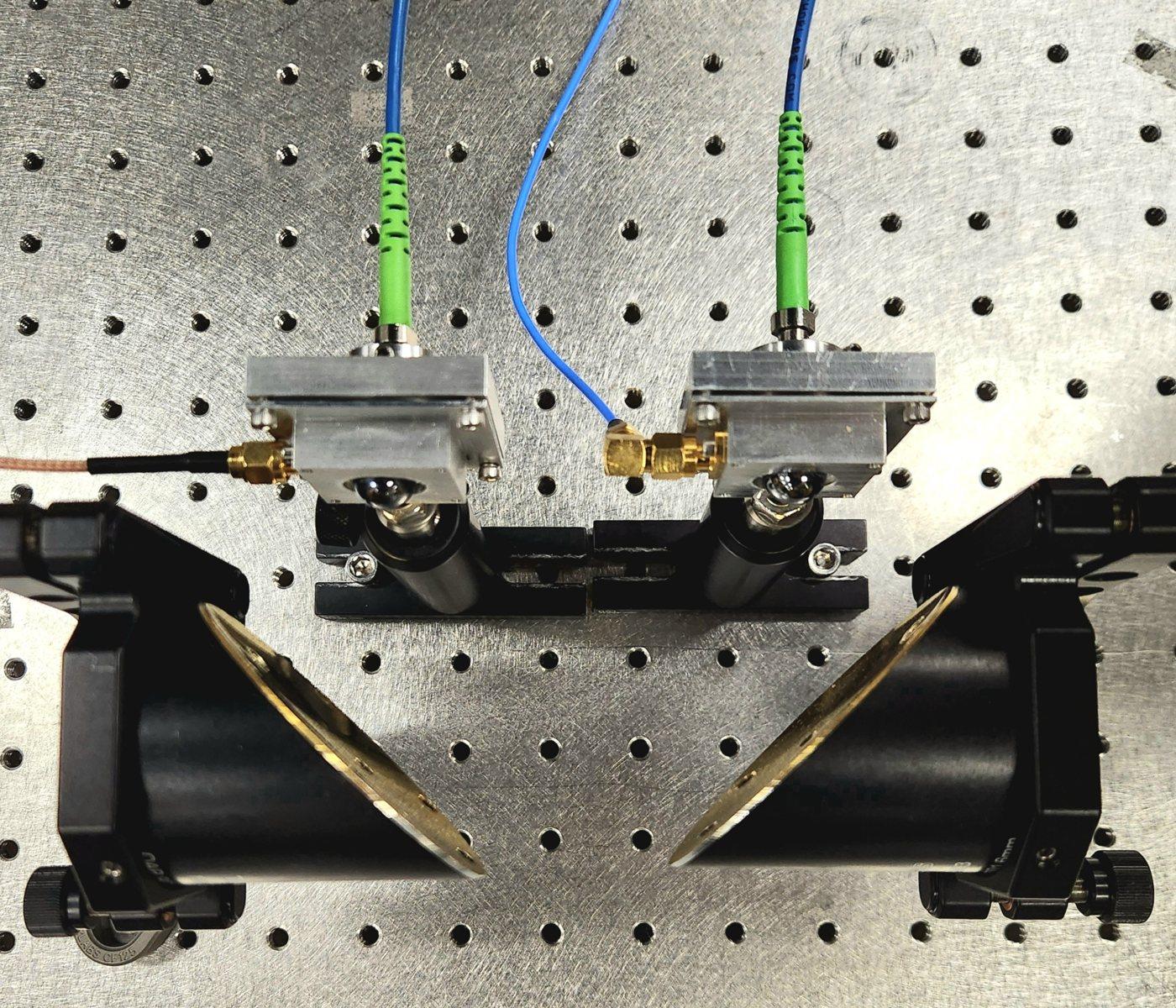
Detector arrays image many points at once, replacing slow point-by-point raster scanning and enhancing imaging throughput more than 1000 times.
High SNR, Wide Bandwidth
More than 1,000 times higher dynamic range than conventional THz-TDS systems, enabling cleaner signals, imaging through more lossy environments, and shorter measurement times.
Hyperspectral Imaging
Every pixel captures a rich terahertz spectral fingerprint, revealing hidden material composition beyond the reach of conventional imaging systems.
3D Imaging
Terahertz echoes from buried interfaces reveal hidden 3D structures, enabling precise measurements of layer thicknesses and subsurface features without cutting the sample.
Advanced Data Analysis Solutions
Software transforms complex terahertz waveforms into actionable insights on material composition, layer thickness, and hidden defects, enabling precise, automated quality control in real time.
Products
Single-pixel terahertz scanners
Multi-pixel terahertz scanners
Solutions
Offering in-line/in-situ quality control solutions for advanced manufacturing
A single, non-contact, in-line measurement provides comprehensive insights into multiple quality parameters simultaneously.
Defect detection
Non-contact detection of surface and subsurface defects, including hidden flaws.
Thickness measurement
Precise, non-contact measurement of coating and layer thicknesses using terahertz pulse time delays.
Material characterization
Comprehensive assessment of material density, uniformity, and internal structure throughout the component.
Chemical identification
Identification of chemical composition and material properties through unique terahertz spectral fingerprints.
Porosity evaluation
Sensitive detection and characterization of voids and pore structures within coatings and material layers.
Conductivity determination
Non-contact measurement of electrical conductivity without physical probes or electrodes.
Publications
Selected publications
Work from our team since 2021.
Journal articles
- 2024
Plasmonic photoconductive terahertz focal-plane array with pixel super-resolution
X Li, D Mengu, NT Yardimci, D Turan, A Charkhesht, A Ozcan, M Jarrahi
Nature Photonics 18, 139-148
- 2023
Rapid sensing of hidden objects and defects using a single-pixel diffractive terahertz sensor
J Li, X Li, NT Yardimci, J Hu, Y Li, J Chen, YC Hung, M Jarrahi, A Ozcan
Nature Communications 14, 6791
- 2023
Low baseline intraspecific variation in leaf pressure-volume traits: biophysical basis and implications for spectroscopic sensing
M. Browne, M. Bartlett, C. Henry, M. Jarrahi, G. John, C. Scoffoni, N. T. Yardimci, L. Sack
Physiologia Plantarum 175, e13974
- 2022
P.-K. Lu, A. Fernandez Olvera, D. Turan, T. S. Seifert, N. T. Yardimci, T. Kampfrath, S. Preu, M. Jarrahi
Nanophotonics 11, 2661-2691
- 2021
Wavelength conversion through plasmon-coupled surface states
D. Turan, P. K. Lu, N. T. Yardimci, Z. Liu, L. Luo, J.-M. Park, U. Nandi, J. Wang, S. Preu, M. Jarrahi
Nature Communications 12, 4641
- 2021
Efficient photoconductive terahertz detection through photon trapping in plasmonic nanocavities
N. T. Yardimci, D. Turan, M. Jarrahi
APL Photonics 6, 080802
Conference talks and proceedings
- 2026
From Laboratory to Production: Deployable Terahertz Scanning for High-Volume Manufacturing
N. T. Yardimci, M. Jarrahi
SPIE Photonics West, San Francisco, CA (invited)
- 2025
Plasmonic nanoantenna-based terahertz focal plane arrays for high-speed multi-pixel imaging
N. T. Yardimci, A. Charkhesht, G. Pawin, S. Recinos, M. Jarrahi
SPIE Optics + Photonics, San Diego, CA (invited)
- 2025
Advancing terahertz pulsed imaging: a multi-pixel approach using plasmonic nanoantennas
N. T. Yardimci, A. Charkhesht, M. Jarrahi
SPIE Photonics West, San Francisco, CA (invited)
- 2024
Rapid scanning through wide field-of-view terahertz focal plane arrays
N. T. Yardimci, A. Charkhesht, D. Turan, M. Jarrahi
SPIE Optics + Photonics, San Diego, CA (invited)
- 2024
Mitigating saturation effects in photomixer-based terahertz receivers with plasmonic nanoantenna arrays
J. Hwang, S. A. Tsao, N. T. Yardimci, M. Jarrahi
Proc. SPIE Optics + Photonics, San Diego, CA
- 2024
High-throughput terahertz scanning for quality assessment of battery electrode manufacturing
N. T. Yardimci, A. Charkhesht, M. Jarrahi
SPIE Smart Structures + Nondestructive Evaluation, Long Beach, CA (invited); Proc. SPIE 12951, 129510P
- 2024
High-Speed and Large Field-of-View Imaging through Terahertz Focal Plane Arrays
N. T. Yardimci, D. Turan, A. Charkhesht, M. Jarrahi
SPIE Photonics West, San Francisco, CA (invited)
- 2023
Terahertz focal plane arrays for high-speed and large field-of-view terahertz imaging
N. T. Yardimci, D. Turan, A. Charkhesht, M. Jarrahi
SPIE Optics + Photonics, San Diego, CA
- 2023
One-Dimensional Terahertz Focal Plane Arrays based on Plasmonic Nanocavities for Terahertz Line Scanning
N. T. Yardimci, D. Turan, A. Charkhesht, M. Jarrahi
SPIE Photonics West, San Francisco, CA
- 2021
High-Switching Contrast Plasmonic Nanocavities for Terahertz Detection with Extremely High Efficiency
N. T. Yardimci, D. Turan, M. Jarrahi
Proc. International Conference on Infrared, Millimeter, and Terahertz Waves, Chengdu, China
- 2021
Broadband Terahertz Detection with 100 dB Dynamic Range through a High Switching-Contrast Plasmonic Nanocavity
N. T. Yardimci, D. Turan, M. Jarrahi
IEEE Microwave Symposium Digest, Atlanta, GA
- 2021
Super-Efficient Terahertz Detection Through High Switching-Contrast Plasmonic Nanocavities
N. T. Yardimci, D. Turan, M. Jarrahi
Proc. Conference on Lasers and Electro-Optics, San Jose, CA
- 2021
High switching contrast photoconductive terahertz detectors based on plasmonic nanocavities
N. T. Yardimci, M. Jarrahi
SPIE Photonics West, San Francisco, CA
- 2021
Fiber-coupled terahertz source based on passive transponder nanoantennas
D. Turan, N. T. Yardimci, P. K. Lu, M. Jarrahi
Proc. SPIE Photonics West, San Francisco, CA
Acknowledgments
Thank you to our sponsors
Our technology has been developed with the support of the U.S. Department of Energy, the Office of Naval Research, the U.S. Air Force, the National Aeronautics and Space Administration, and the California Energy Commission. We are grateful for their trust in our work.
Contact
Contact us
Tell us about your material, process or inspection challenge and we will get back to you by email.
- info@lookininc.com
- Office and lab
- 5839 Green Valley Cir., Ste. 205
Culver City, CA 90230